
Applied Materials intends to establish an engineering centre in India and create goods that will increase total profits 2023

Applied Materials intends to establish an engineering centre in India and create goods that will increase total profits 2023
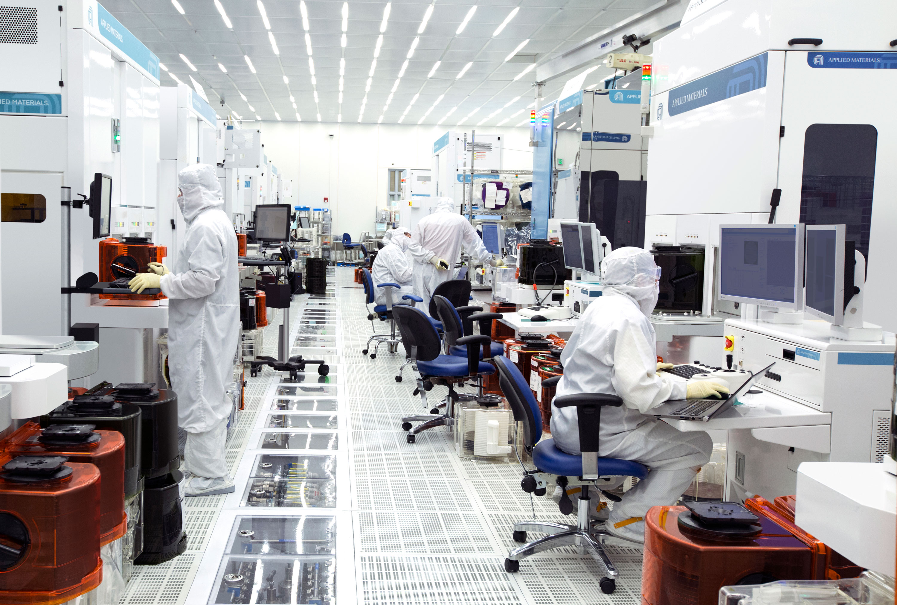
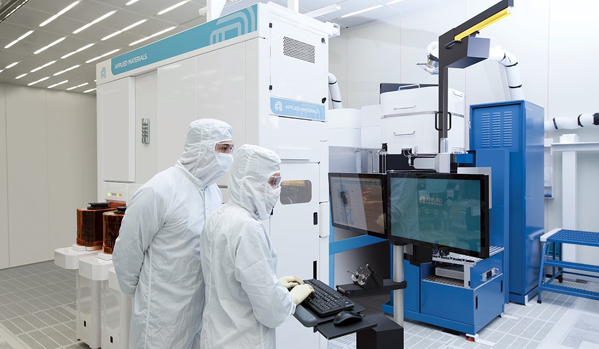
Last month, Applied Materials said it would invest $400 million over four years to create an engineering facility in Bengaluru, focusing on developing and marketing technology for the semiconductor manufacturing industry.
On Friday, Applied Materials, a semiconductor equipment manufacturer, claimed that its intention to establish an engineering department in India and develop products will help increase its total margins internationally.


Prabu Raja, president of Applied Materials’ Semiconductor Products Group, said, “We are investing in India because of the reduced cost and time involved in creating the products and solutions for the semiconductor manufacturers. “Time is significant and is worth billions of dollars, and we are convinced that time and cost are better in India.”
According to him, the advantages will result in “boosted margins once the products are developed at scale in its manufacturing facilities around the world.” The priority for Applied Materials in India would be first to create a few goods or their prototypes, following which it will be possible to assess if it would be feasible to sell them. The items may then be produced in large quantities at Singapore and Austin, Texas factories in the United States.
According to Raja, India is a significant market for the R&D, design, creation and testing of goods and talent. “At this point, we are not looking at manufacturing in India on a larger scale as we already have an ecosystem and our facilities in other places outside India,” Raja added. The business has groups for product development, R&D, IT, and operational skills, and it now has six facilities in India.
Last month, Applied Materials said it would invest $400 million over four years to create an engineering facility in Bengaluru, focusing on developing and marketing technology for the semiconductor manufacturing industry.
The startup wants to create five to six original items at first for the Indian industry. Products for both cutting-edge and older semiconductor nodes will be developed by it.
Raja withheld information on the kinds of goods and services that would be created in India. The Plasma Abatement System, which lowers the high global-warming potential (GWP) of the gaseous chemicals used, Aeris-Si, which is used for subfab fireline cleaning to manage silica load and improve pump lifetime, and products for cleaning methods for chip processes are just a few of the essential products for the semiconductor industry that Applied Materials has developed.
“We hope to finish setting up the construction infrastructure soon. The suppliers and necessary equipment must then be gathered, according to Raja.
As of the fiscal year that concluded in October 2022, Applied Materials recorded $25.8 billion in yearly sales. The business has made a $2.8 billion investment in R&D. There are 17,300 active patents currently.
Applied Materials, the leading semiconductor and display equipment manufacturer, recently announced plans to establish an advanced engineering centre in India as a part of its global expansion strategy. This move is anticipated to bolster Applied Materials’ position as a technological innovator in the semiconductor sector, bringing it closer to the rapidly evolving Indian market and contributing to overall margin growth in 2023.
The upcoming centre will be located in Bangalore, India, which is recognized as the “Silicon Valley of India” and is a renowned technology hub. By leveraging India’s vast engineering talent pool, Applied Materials aims to expedite its research and development (R&D) processes and drive new product innovation.
One of the primary goals of the proposed engineering centre is to work towards the development of more efficient and cost-effective manufacturing solutions. These solutions will cater to global and local markets and give Applied Materials a competitive edge, propelling its growth trajectory.
Applied Materials’ decision to establish a dedicated engineering centre in India is part of a larger strategic plan to bolster overall margins. The company aims to reduce operating costs and improve profit margins by creating products that simplify production and increase manufacturing yield.
The centre will focus on enhancing current products and developing new, more efficient equipment that can improve throughput, yield, and cost of ownership. It is anticipated that these new products will offer substantial operational improvements to customers, which in turn is expected to drive higher product demand and revenue for Applied Materials.
The decision to set up an engineering centre in India aligns with the country’s expanding tech landscape. As a leading tech hub in Asia, India provides a conducive environment for tech giants like Applied Materials to thrive and grow.
Moreover, by setting up a local engineering centre, Applied Materials can directly tap into the local semiconductor and display equipment markets. The Indian government’s efforts to boost local manufacturing through various initiatives, such as the Production-Linked Incentive (PLI) scheme, further underscore the potential of this strategic move.

Creating an engineering centre in India will also allow Applied Materials to tackle the emerging challenges in the semiconductor industry more effectively.
The technology industry is quickly moving towards advanced technologies such as the Internet of Things (IoT), Artificial Intelligence (AI), and 5G communication. This requires semiconductors that are more powerful and efficient. By leveraging local expertise and understanding of these sectors, Applied Materials will be better positioned to develop products that meet these emerging demands.
Applied Materials’ strategic move to set up an engineering centre in India marks a significant milestone in the company’s global expansion strategy. The company aims to expedite its product innovation and enhance its overall margins by leveraging India’s technical talent and booming tech sector.

The new centre is poised to drive growth for the company in 2023 and beyond, reinforcing Applied Materials’ position as a global leader in semiconductor and display equipment manufacturing.