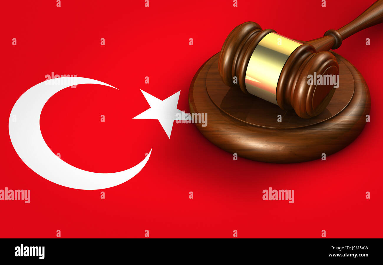
Turkey passes a law that will facilitate Government control of Social Media
The law will force companies like Twitter, Facebook, and YouTube to settle their servers in the Eurasian country, something that will facilitate censorship, according to critics.
The law passed by Turkey
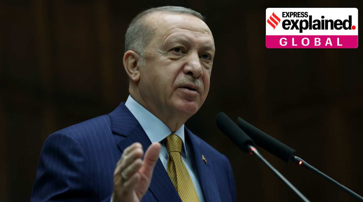
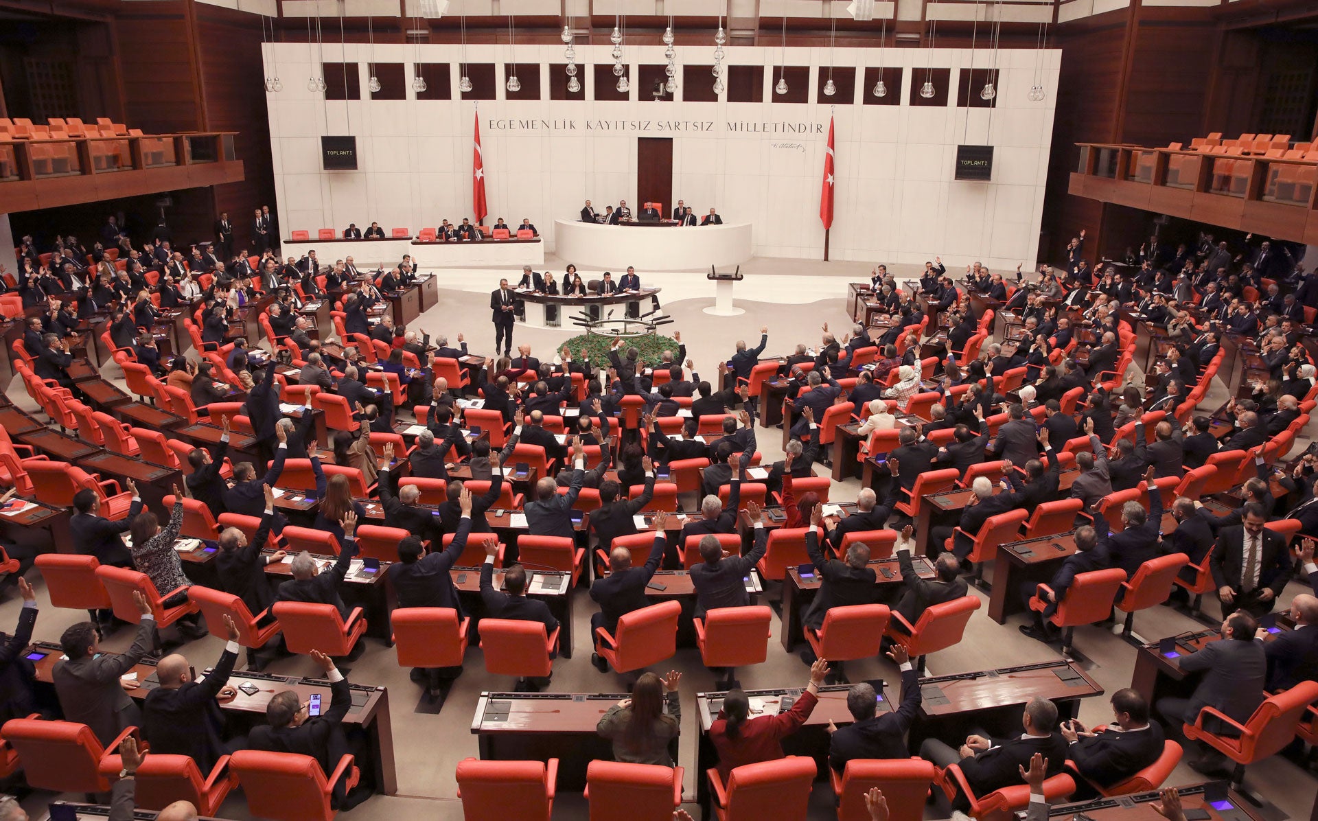
The Turkish Parliament approved a law on Wednesday that tightens the government’s control over social networks and, according to critics, will facilitate censorship. It is one more step for the Islamist President Recep Tayyip Erdogan to dominate the network at a time when many Turkish citizens who distrust the media increasingly linked to the Executive use social networks to inform themselves, especially the younger ones. Erdogan recently said that his position contrary to these platforms is due to the need to “remove all these immoralities from the midst.”
Any digital provider that has more than a million daily visits from Turkey and allows the interaction of its users and publicly share texts, audios, or videos, will be affected by the new legal text. Fundamentally these are companies like Twitter, Facebook, YouTube, or TikTok, which must designate a Turkish citizen as their legal representative in Turkey. The said representative must respond within 48 hours to executive or judicial orders to withdraw content under penalty of fines between 122,000 and 1.22 million euros. Companies that do not appoint such a representative will see their bandwidth reduced by up to 90%.
“Social media is a lifeline for many people who use it to access news so, this law will signal a new and dark era of censorship” Tom Porteous of the NGO Human Rights Watch denounced Tuesday before the vote”. Social media companies should loudly and clearly demand that Turkey withdraw this law and the European Union should support this appeal”, he added.
One of the most controversial issues of the new regulation is that it requires social networks to keep part of their servers in Turkey and host all the data generated by Turkish users there, which will facilitate “the erasure of digital memory”, according to affirmed these days the lawyer Gülsah Deniz-Atalar, expert in law and information technology. In this way, thorny issues for the Executive, such as the corruption accusations made a few years ago could vanish from the web.
The pro-government deputies justify the new measures in the need to guarantee the “right to be forgotten” and prevent “defamation” campaigns, but no one escapes that what is sought is to reduce the spaces in which citizens can express themselves more freely and share the news. The text has been approved with the votes of the formation of Erdogan, the Islamist Justice and Development Party (AKP), and its far-right partner Nationalist Action Party (MHP).
The latter had come to propose even tougher measures, such as the need that every account on social networks should be linked to a Turkish identity document. Finally, this has been discarded perhaps not only because of its technical difficulty but also because thousands of anonymous accounts are used as trolls by the government party to harass the most critical commentators. In fact, on June 11, Twitter suspended more than 32,000 accounts used to manipulate public discourse linked to the governments of China, Russia, and Turkey. 7,000 of them were tied to the AKP.
To get an idea of the effects of the new law, just look at the latest transparency report on Twitter, which covers the first half of 2019. Turkey was the country that presented the most demands for content removal; 6,073 requests on almost 9,000 accounts. But the US-based company only agreed to delete 5% of its content. Nor did it provide information on nearly 600 accounts from which Ankara requested it. Now, with the new text, Twitter should agree to delete all the requested content and provide information about the accounts that the Turkish Government requires.
According to an organization Engelliweb, at the end of 2019 access to 130,000 URLs were blocked from Turkey, as well as 7,000 Twitter accounts, 40,000 tweets, 10,000 YouTube videos, and 6,200 Facebook content. Access to YouTube and Facebook has also been blocked several times over the past decade, although many users chose to circumvent censorship using VPN.
However, the lawyer Kerem Altinparmak maintains that the rush to write the new law and its poor language allow gaps to avoid censorship. It would be enough, according to this human rights expert, that the companies comply with the part of appointing a representative in Turkey, without even establishing their servers in the country, and alleging that the content that the government demands to remove is protected by freedom of expression laws.